Advanced (S)TEM and In Silico Investigation of Oxide-based MIM Heterostructure Devices
Project Members: Tianshu Jiang (PhD Student), Leopoldo Molina-Luna (PI)
Description:
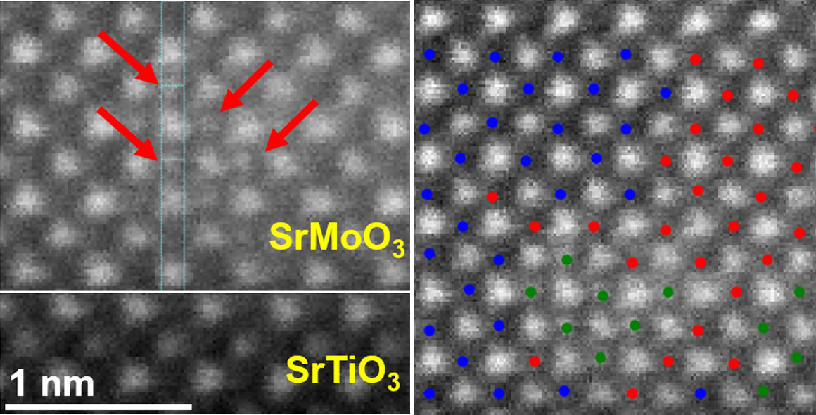
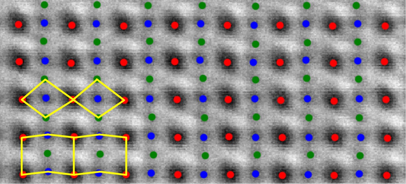
Interfacial engineering at the atomic level provides possibilities to optimize the electrical properties of tunable oxide-based metal-insulator-metal (MIM) heterostructure devices.
For example, the interfaces between various bottom Scandate-electrodes, a SrTiO3 (denoted as STO) buffer layer and a highly conducting layer SrMoO3 (denoted as SMO) are currently investigated by using a set of novel electron microscopy techniques such as HAADF-STEM, ABF-STEM, 4D-STEM and machine learning based modelling.
By doing this, we aim to obtain structure-property correlations to directly link the atomic structure (defects, strain and local lattice distortions) with the macroscopic electrical properties.