


Advanced Electron Microscopy Division
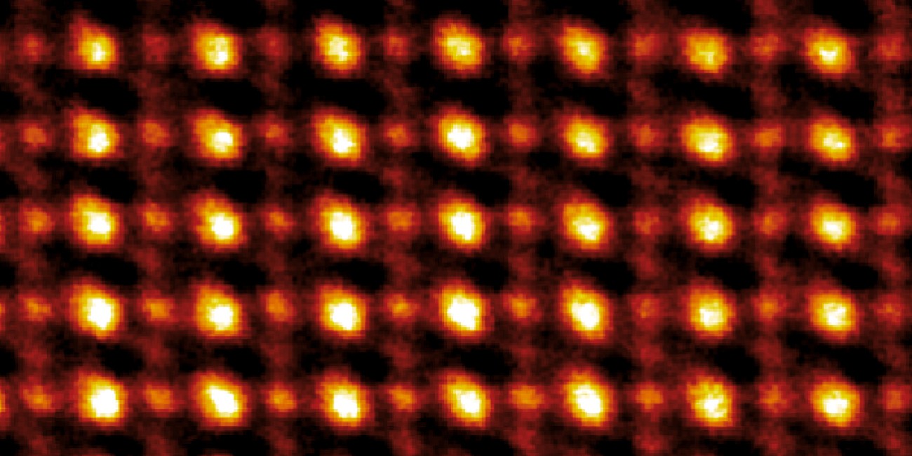
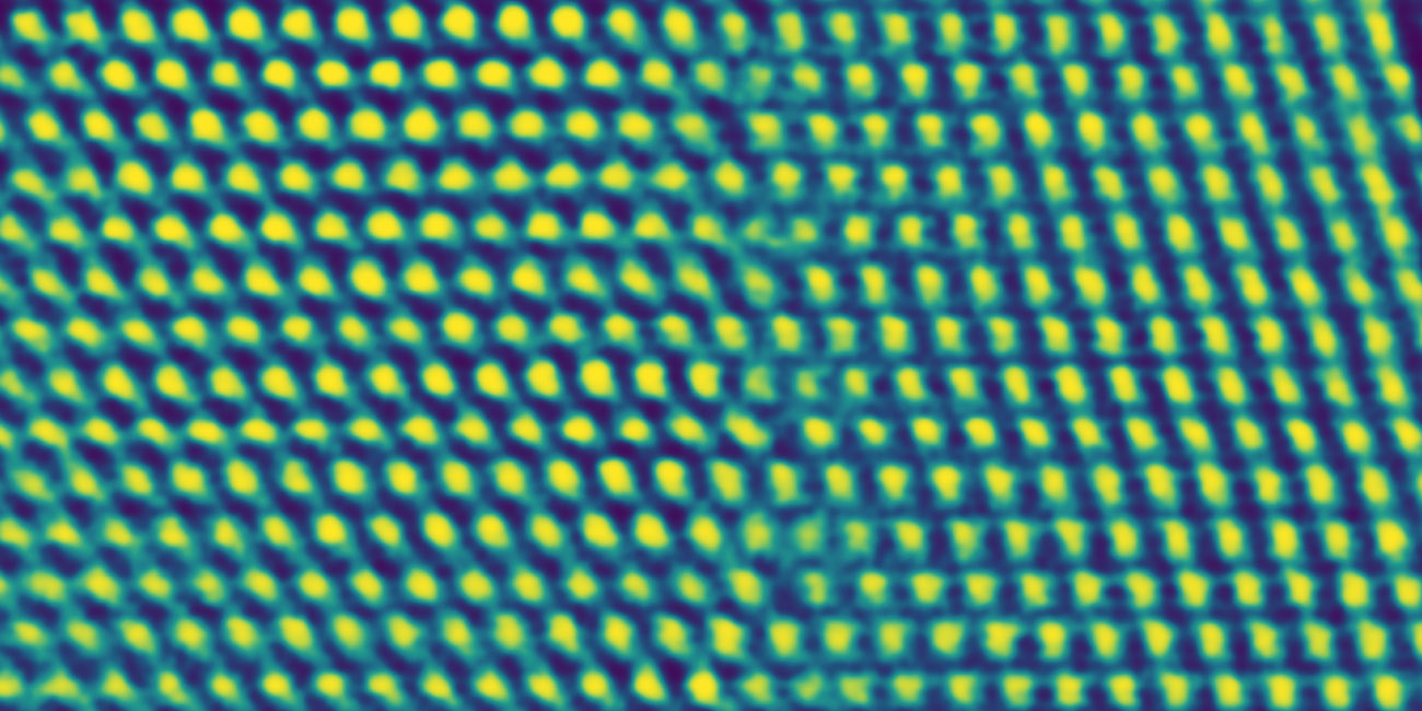
The mission of the European Research Council (ERC) funded Advanced Electron Microscopy (AEM) Division at TU Darmstadt is to establish atomic-scale structure-property correlations in functional materials and devices. Based on our expertise in aberration-corrected scanning transmission electron microscopy for atomic-resolution imaging and analysis in Materials Science, we aim to develop and apply state-of-the-art in situ/operando (S)TEM for stimuli-based studies ( i.e. temperature, electrical biasing, gas and cooling). A further direction will be the implementation and application of 4D-STEM. We have also a strong interest in big data analysis for EM. The group has a broad international collaborations network in Science and Industry.
Our group is located in the research field M+M (Matter and Materials) of the TU Darmstadt.
Prof. Molina-Luna is Head of the In Situ Microstructural Analytics Lab (InSituLab) of the Center for Reliability Analytics (CRA), TU Darmstadt

Head of the Division
Prof. Dr. Leopoldo Molina-Luna Tel. +49 6151 16-20180 Fax. +49 6151 16-20185 Peter-Grünberg-Straße 2 D- 64297 Darmstadt Raum: L2|01 52


Opening of the iJRL Memristor Technology and NCKU-TUDa Workshop on Memristor Technology -from material to energy efficient computing
Prof. Molina-Luna was part of the TUDa delegation to Taiwan and delivered a talk at the NCKU-TUDa Workshop.
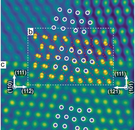
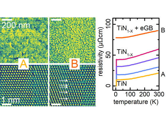
The iJRL „Memristor Technology“ pursues the goal to progress on relevant aspects of the fundamentals, technology and exploitation of memristive devices. It addresses the materials properties and defect structure of several kinds of memristor realizations based on oxide, magnetic and ferroelectric materials. From the application side, it covers several novel computing schemes using memristors to increase energy efficiency, including field programmable gate arrays (FPGAs), neuromorphic computation and processing-in-memory. From the analysis and modelling side, a unique selling point is to encompass all relevant scales from density functional theory, multi-phase and compact modelling as well as circuit design. The experimental analysis correlates advanced transmission electron microscopy (TEM) methods with physical models used for compact simulation of model device and array behavior. Thereby, the iJRL establishes a methodology from innovative materials to single devices and arrays up to the circuit level that can be transferred to novel emerging materials in this fast-developing field also for interested partners in the field of electronic material and semiconductor industry.

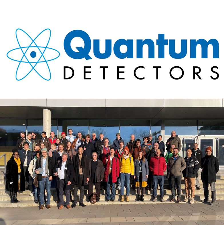
Quantum Detectors and NanoMEGAS seminar with Technische Universität Darmstadt (Advanced Electron Microscopy Division)
Tuesday 28th February 2023 at 4pm – 6pm
Quantum Detectors and NanoMEGAS would like to invite you to a seminar and a live demonstration of the MerlinEM and NanoMEGAS DigiSTAR precession hardware showcasing 4D STEM and precession in association with Technische Universität Darmstadt (TU Darmstadt).
This event will see talks from all three institutions, Quantum Detectors, NanoMEGAS and TU Darmstadt. Prof. Dr. Leopoldo Molina-Luna's group will give a live demonstration of their JEOL ARM-200F showing the capabilities of the MerlinEM alongside the NanoMEGAS DigiSTAR precession hardware. You will also be granted VIP behind-the-scenes access to view the TU Darmstadt lab and the JEOL ARM-200F.
This will run alongside those attending the Microscopy Conference in Darmstadt and as a virtual event in case you cannot make it to Darmstadt. Quantum Detectors will also be exhibiting at MC Darmstadt 2023.
We hope to see you there. Sign up below!
Sign up link: https://forms.gle/DLvF2onJV49WmiVG8
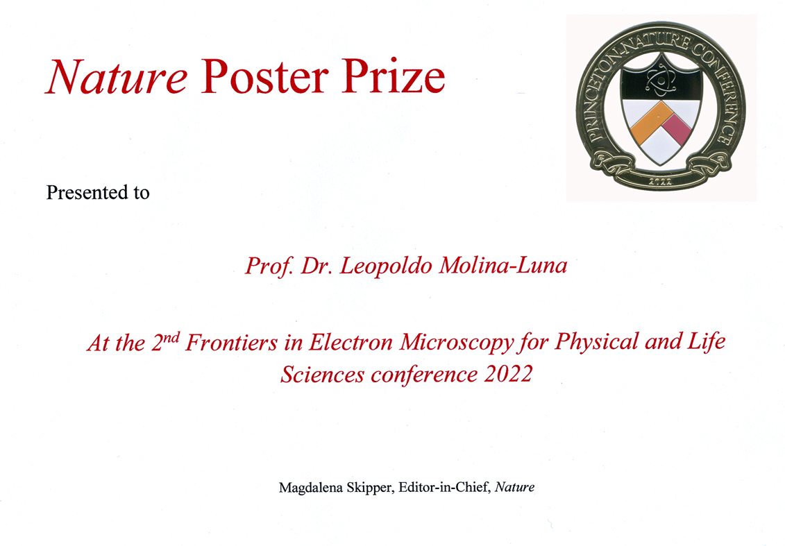
Poster Prize for Physical Sciences at the Princeton-Nature 2nd Frontiers in Electron Microscopy for Physical and Life Sciences Conference 2022
This certificate is in recognition of the poster prize awarded to Leopoldo Molina-Luna at the 2nd Frontiers in Electron Microscopy for Physical and Life Sciences Princeton-Nature conference, held Sept 28-30 2022. In recognition of a flash talk and poster presentation of his lab’s work, Leopoldo was provided with a 1 year subscription to Nature, the international journal of science.
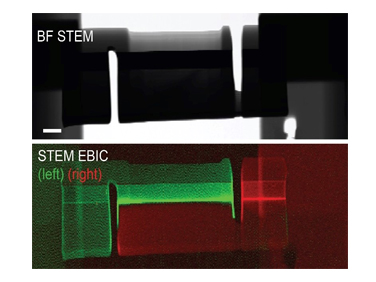
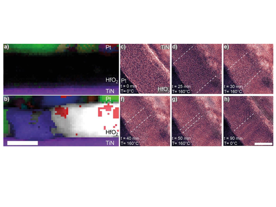
OPERANDO TWO-TERMINAL DEVICES INSIDE A TRANSMISSION ELECTRON MICROSCOPE
Oscar Recalde-Benitez1, Tianshu Jiang1, Robert Winkler1, Alexander Zintler1, Yating Ruan2, Esmaeil Adabifiroozjaei1, Alexey Arzumanov2, Tijn van Omme3, William A. Hubbard4,5 Yevheniy Pivak3, Hector H. Perez-Garza3, B. C. Regan 4,5, Philipp Komissinskiy2, Lambert Alff2 and Leopoldo Molina-Luna1*
1. Advanced Electron Microscopy Division, Department of Materials- and Earth Science, Technical University of Darmstadt, Darmstadt, Hessen, Germany.
2. Advanced Thin Film Technology Division, Department of Materials- and Earth Science,Technical University of Darmstadt, Darmstadt, Hessen, Germany.
3. DENSsolutions, Delft, Netherlands.
4. NanoElectronic Imaging, Inc., Los Angeles, CA, USA.
5. University of California, Los Angeles and the California NanoSystems Institute, Los Angeles, USA.


Contact
Prof. Dr. rer. nat. Leopoldo Molina-Luna

molina@aem.tu-...
work +49 6151 16-20180
Work
L2|01 52
Peter-Grünberg-Strasse 2
64287
Darmstadt