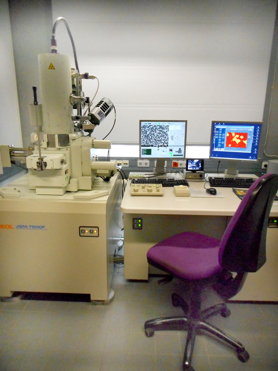
The JEOL JMS 7600F
is a high-resolution SEM with various imaging options (in-lens SE, BSE, STEM). The near-sample position of the BSE detector allows chemical contrast imaging up to high magnifications. The high count rate of the EDX detector enables element mappings in a short time.
Installation: 2011
Resolution: 1.0 nm (15 kV) – 1.4 nm (1.0 kV)
Equipment:
- Field emission cathode (Schottky)
- in-lens SE detector
- BSE detector
- EDX detector (SDD-X-Max 80, Oxford)
- STEM detector
The JEOL JIB 4600F scanning electron microscope (SEM)
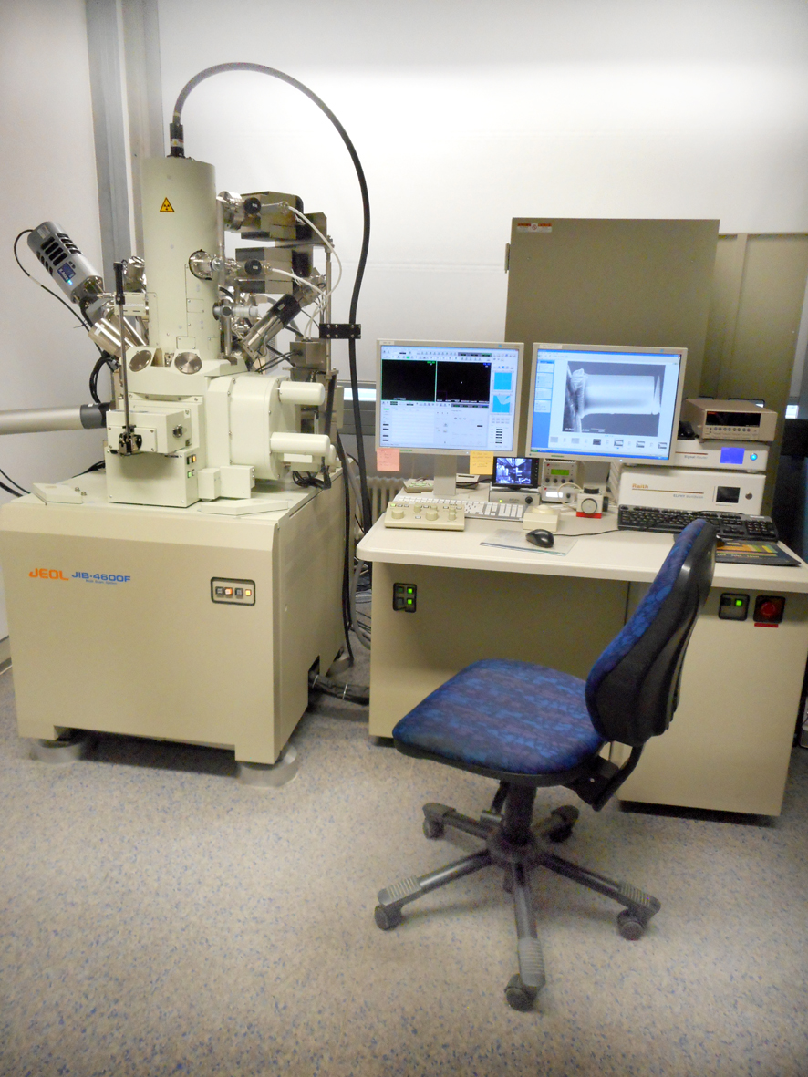
is a dual-beam FIB in which the sample can be imaged in parallel to ion thinning or processing. Equipped with an EDX detector, an EBSD unit, a Kleindiek micromanipulator and an electron lithography unit, the FIB allows targeted TEM sample preparation, film lift-out and local material characterization (imaging, analysis and diffraction).
Installation: 2012
Resolution: 1.2 nm (30 kV, SEM), 5.0 nm (30 kV, SE/Ga ions)
Equipment:
- Field emission cathode (Schottky)
- in-lens SE detector
- BSE detector
- EDX detector (INCA Energy 350, Oxford)
- Micromanipulator (triaxial, Kleindiek)
- Gas inlet systems (Pt, C)
- Lithography system (Elphy Plus, Raith)
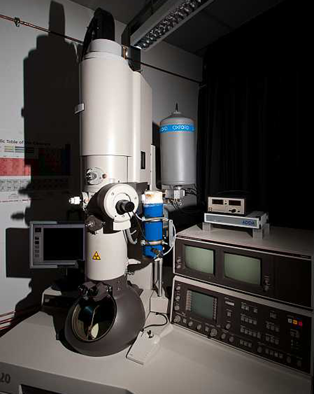
TEM – FEI CM20 ST
the CM20 is a very reliable TEM for routine applications and is also used in student training. Equipped with a LaB6 cathode, an EDX system and a STEM unit, it is used for the chemical and structural investigation of many material systems. A range of holder systems are available to enable in-situ E-field investigations, among other things.
Installation: 1993
Resolution: 2.3 Å (TEM, 200 kV)
Equipment:
- LaB6 cathode
- BF, DF, diffraction
- STEM unit
- Single tilt holder
- Be double tilt holder
- Double tilt holder (cooled)
- E-field holder (SFB 595; self-made)
- EDX detector (SDD-X-Max 80, Oxford)
- CCD camera
The JEOL JEM 2100F TEM
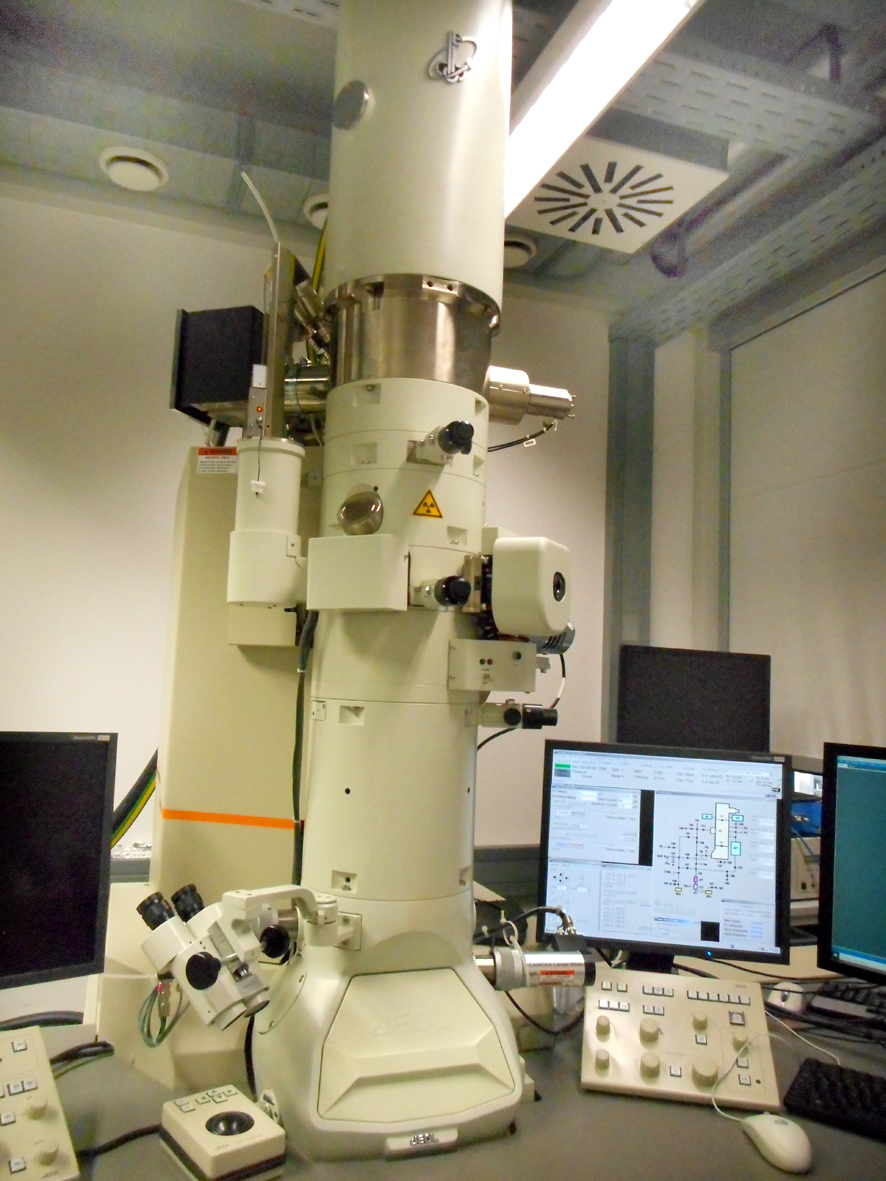
is available to a broad user group, especially for routine applications. In addition to conventional TEM (BF, DF, SAED), a STEM unit in combination with an SDD-EDS detector enables chemical investigations with higher resolution and high count rates.
Installation: • 2011
Resolution: • 2.2 Å (TEM, 200 kV)
Equipment:
• Field Emission Cathode (Schottky Emitter)
• EDS-Detector (X-Max 80 SDD Detector, Oxford)
• DF, HAADF, BF
• Be Double Tilt Holder
• Ta Double Tilt Heater Holder (1000°C)
• Single Tilt Holder
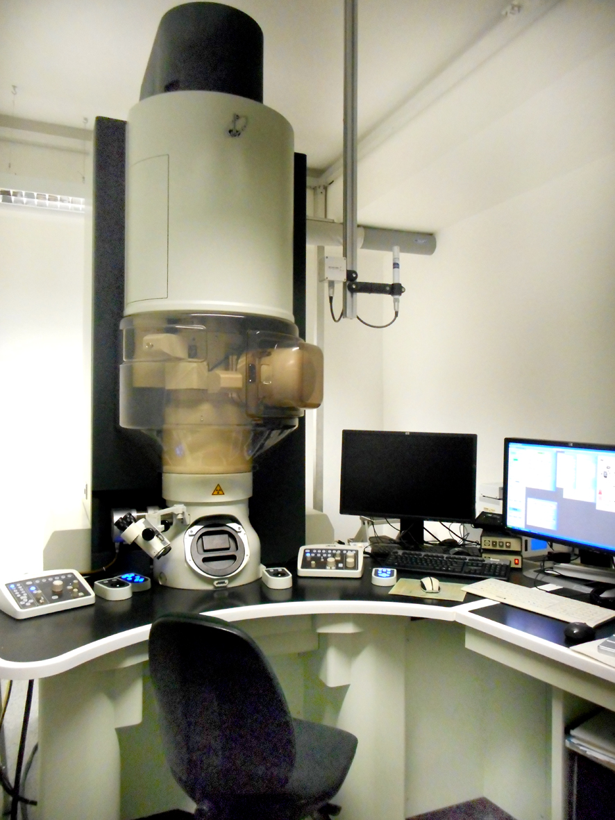
The ARM 200F
enables imaging and chemical characterization on the atomic scale by correcting the spherical aberration (Cs) of the condenser system. Main applications are therefore the characterization of interfaces, phase boundaries, crystal defects as well as highest resolution chemical investigations by EELS and EDS.
Installation: • 2011
Resolution: • 0.8 Å (STEM); 1.9 Å (TEM, 200kV)
Equipment:
• Field Emission Cathode (Schottky Emitter)
• Cs-corrector (Condenser System)
• EELS Detector (Gatan Enfina)
• EDS Detector (JED 2300T, JEOL)
• DF, HAADF, BF, ABF
• Stabilized Be Double Tilt Holder
• Single Tilt Holder
• In situ TEM Biasing & Heating – DENSsolutions Lightning
• In situ TEM Gas & Heating – DENSsolutions Climate