Correlating the influence of microstructure and grain boundaries on electric properties in thin film oxide RRAM devices – a component specific approach
Project Members: Alexander Zintler(PhD Student), Leopoldo Molina-Luna (PI)
Description:
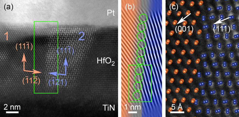
Valence change memory (VCM) based resistive random-access memory (RRAM) devices are promising candidates in the field of highly scalable, non-volatile and neuromorphic memory alternatives. Although extensive research is performed on the macroscopic, electronic properties of these thin film devices, an atomistic understanding of the resistive switching process is still lacking. The focus of this work is on the structural and morphological features that are inherent in the 10 nm oxide thin film of the metal-insulator-metal (MIM) stack. The nanoscale microstructure of the films locally changes the electrical properties and consequently the properties of the complete device. Features such as grain boundaries present localized high defect concentration volumes that directly influence the electroforming (as well as set and reset) behavior of memory device. To understand in detail, which type of grain boundaries are present in the thin films, a set of high-resolution STEM methods are applied to collect datasets that allow the determination of the phase and orientation of the Hafnia grains in the thin film at nanometer scale. As the morphology is strongly affected by the deposition parameters during thin film growth and the texture of the substrate or preceding thin film, the Titanium Nitride bottom electrode is included in the investigations of the morphology of the full MIM stack. Cross-sectional sample preparation of the thin film devices allows atomic-resolution HAADF imaging, where grain boundary recombination behavior is investigated and form a crucial input parameter for DFT simulation approaches that address these complex structural features. Direct electron detection based 4D-STEM allows the direct mapping of the orientations of all grains at nanometer resolution over large areas of interest (500*500 nm²). Automated crystal orientation mapping (ACOM) can be applied on the cross-sectional samples, as well as on plan-view samples, to achieve a high number of sampled grains. Machine learning based data treatment opens an additional path of handling the datasets and differentiating between phases and orientations with reduced user input. The component specific approach, together with the three-dimensional understanding of the thin film morphology of the full device stack, gives a unique, high-resolution understanding of the present devices and helps to optimize Hafnia based RRAM devices from growth parameter selection to device integration.
Petzold, Stefan, Alexander Zintler, Robert Eilhardt, Eszter Piros, Nico Kaiser, Sankaramangalam Ulhas Sharath, Tobias Vogel, et al. “Forming-Free Grain Boundary Engineered Hafnium Oxide Resistive Random Access Memory Devices.” Advanced Electronic Materials 5, no. 10 (2019): 1900484.link
Zintler, Alexander, Robert Eilhardt, Shuai Wang, Matus Krajnak, Patrick Schramowski, Wolfgang Stammer, Stefan Petzold, et al. “Machine Learning Assisted Pattern Matching: Insight into Oxide Electronic Device Performance by Phase Determination in 4D-STEM Datasets.” Microscopy and Microanalysis, Volume 26, Supplement S2, August 2020, pp.1908-1909.link
GEPRIS entry of the DFG project: link