Our main interest lays on on design, fabricate, and manipulate nanostructured materials focusing particularly on TiO2-based nanostructures (e.g., pure, doped, co-doped). By tuning the morphology and composition of nanoparticles and nanoparticle films, we aim to control the mobility of the charge carriers to develop high-performing devices for environmental and energy applications such as water splitting and gas sensing.
- Preparation and characterization of metal-doped/co-doped TiO2 nanostructured materials for
- enhanced photocatalysis
- gas sensing
- Prof. Olim N. Ruzimuradov, Associate Professor, Turin Polytechnic University, Tashkent, Uzbekistan
[1] I. Gonzalo-Juan, L. Mace, S. Tengeler, A. Mosallem, N. Nicoloso, R. Riedel, Photoluminescence of urea- and urea/rhodamine B-capped TiO2 nanoparticles, Materials Chemistry and Physics 177 (2016) 472-478.
[2] M. Hojamberdiev, I. Gonzalo-Juan, Ca-assisted nitrogen-rich molecular approach for the synthesis of monodisperse tantalum oxide and (oxy)nitride nanocrystals for visible light–induced water oxidation, Journal of the Ceramic Society of Japan 124(10) (2016) 1052-1055.
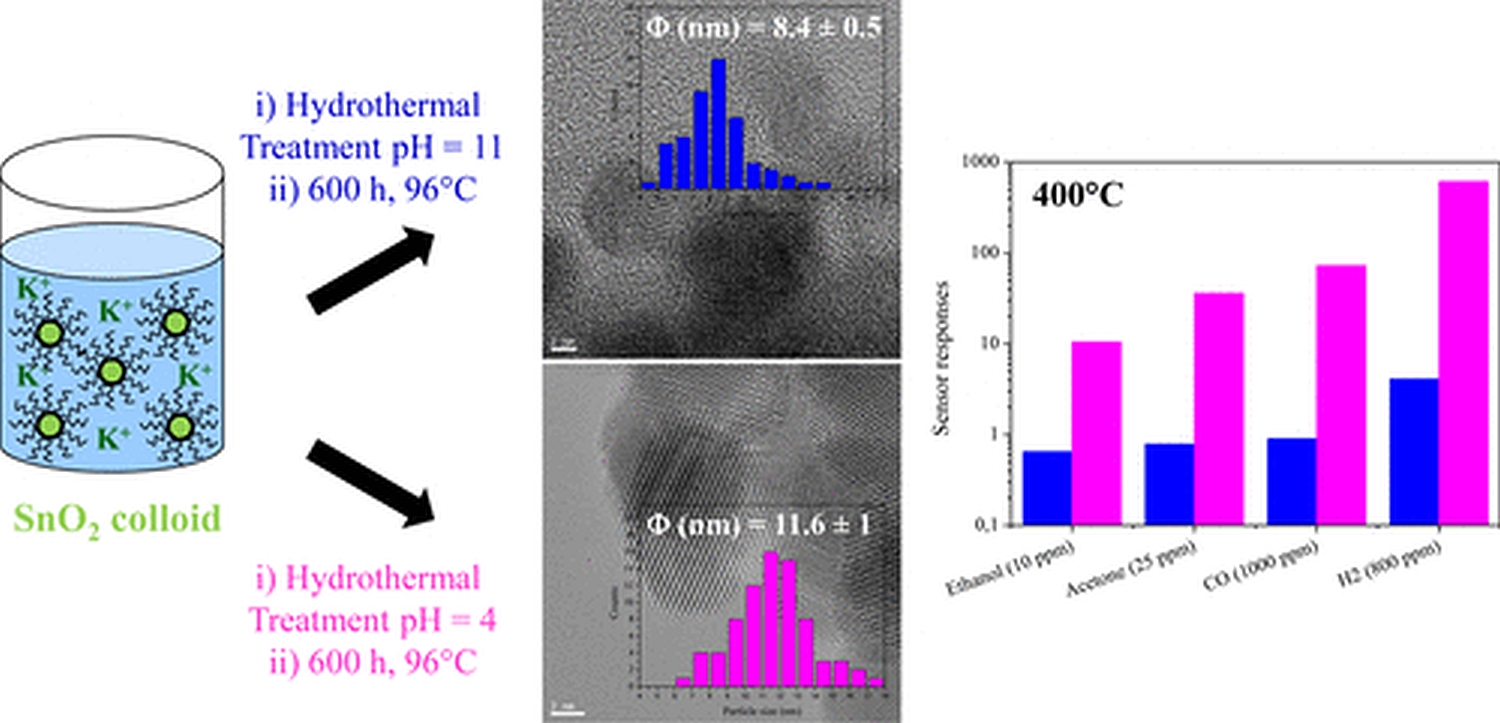
[3] S.H. Lee, V. Galstyan, A. Ponzoni, I. Gonzalo-Juan, R. Riedel, M.A. Dourges, Y. Nicolas, T. Toupance, Finely Tuned SnO2 Nanoparticles for Efficient Detection of Reducing and Oxidizing Gases: The Influence of Alkali Metal Cation on Gas-Sensing Properties, ACS Applied Materials & Interfaces 10(12) (2018) 10173-10184.